This is a simple work based on digital circuits, no programming, no circuit design, just two chips.
This work is especially suitable for beginners. The essence of this work is the heart-shaped lantern made up of digital chip CD4017. The display mode is OK according to your own preferences and creativity. It’s definitely better to make such a gift and give it to her.
First, the parts you need:
DuPont line (several)
2. Universal board X2
3. Potentiometer X2
4. 470uF capacitor X1
5. Diode X4
6. Transformer X1
7. 104 capacitors (several)
8. LM7809 chip X1
9. Heat sink X1
10. Various color LED lights (if available)
11. 100uF capacitor X1
12.2K resistance X1
13. 680 ohm resistor (several)
14. Common Yin Digital Tube X4
15. NE555 and CD4017 (one piece each)
16. Chip base X2 (favorable for secondary use of the chip)
17. 5 pieces of wooden board and 2 pieces of wrapping paper (size depends on your own situation)
The required device is shown below:
I divide the circuit of the work into three parts. These three parts are based on my real object. Of course you can have better ideas to improve it.
First, the power circuit:
Since the positioning of the work is a gift, the power must be installed inside.
The CD4017 has a higher operating voltage, and the lighting environment is indoors, so we consider using AC power. A small transformer of 3~5 watts is enough, and the secondary output of the transformer is required to be 7~8V, so that the 9~10V DC voltage required by the system can be obtained after rectification and filtering.
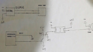
The following is a schematic and physical map of this part:
Second, LOVE type birthday lights:
1. Flow drive circuit:
The role of NE555 and CD4017. The NE555 constitutes an oscillating circuit, and the CD4017 is a counting circuit.
The heart-shaped middle part of the LED produces a flow effect, which is based on the combination of NE555 and CD4017. I will explain the circuit principle in detail for beginners below.
The oscillating circuit is composed of a time base integrated circuit NE555 and C2, C3, R1, R2, etc. (C2 is a delay charging capacitor, C3 is an anti-interference isolation capacitor, R1 and R2 are delay charging resistors, and R2 is a discharging resistor. ).
After power-on, the voltage across the capacitor C2 cannot be abrupt, the voltage of the 2 pin is low, the internal flip-flop of the integrated block NE555 is set, and the 3 pin outputs a high level.
At the same time, since the power supply charges C2 through the resistors R1 and R2, the voltages of pins 6 and 2 are continuously increased. When the potential rises to 2/3 of VCC, the internal flip-flop of the integrated block NE555 is reset, and the output voltage of the 3-pin is output. Flip to low.
At the same time, the discharge tube inside the integrated block NE555 is turned on, that is, the 7-pin is connected to the 1 pin through the internal discharge tube, and the charge stored on the C2 is discharged through the R2 and 7-pin, so that the voltages of the 6-pin and the 2-pin are continuously decreased. When reduced to 1/3 of VCC, the internal flip-flop of the integrated block NE555 is set.
At the same time, the discharge tube inside the integrated block NE555 is cut off, the 7-pin is suspended, and the power supply is charged to C2 through R1 and R2, so that the voltage of the 6-pin and the 2-pin is continuously increased... Thus, the oscillation is formed repeatedly.
The high-level sustain time of the output depends on the charging time constant of the capacitor C2, and the low-level sustaining time of the output depends on the discharge time constant of the capacitor C2. Since R2 ≥ R1, it can be considered that f is charged, and the purpose is to reduce the difference in the time interval in which the lanterns are turned off alternately.
If used in other situations, the course adjusts the parameters of R1, R2, and C2 as needed. In summary, the 3 pin is always in a binary state of high level and low level, so the circuit is also called an unsteady circuit.
The decoding circuit consists of a CD4017 integrated block. The manifold has three inputs (14 pins for 2 clock inputs CP and 13 pins for EN and 15 pins for reset terminal Cr). There are 10 output terminals Q0~Q9 (3 feet, 2 feet, 4 feet, 7 feet, 10 feet, 1 foot, 5 feet, 6 feet, 9 feet, 11 feet).
There is also a carry-end CO, whose function is: When the reset terminal Cr is added with a high level and a positive pulse, the output terminal Q0 is at a high level, and the remaining 9 output terminals Q0 to Q9 are at a low level. The clock output CP counts the rising edge of the input clock pulse and EN counts the falling edge of the clock pulse. The output states of the 10 output terminals Q0 to Q9 correspond to the number of input clocks.
If counting from 0, Q1 becomes high when inputting the first clock pulse, and Q2 becomes high when inputting the second clock pulse... until the 10th clock pulse is input, Q0 becomes Is high.
At the same time, the carry terminal C0 outputs a carry pulse as a clock signal for the next stage count. Cr is the reset terminal and is also the clear terminal. When Cr is input to a high level, the circuit is reset, that is, the output terminal Q0 is at a high level, and Q1 to Q9 are at a low level.
Repeatedly, as long as the binary signal sent from the 3 pin of the integrated block NE555 does not disappear, the CD4017 will convert the binary signal into the decimal signal and the counting operation will be repeated.
In summary, adjusting the variable resistor R2 can change the frequency of the oscillating circuit, reflecting the rate at which the output of the CD4017 is flowing.
2. Layout and working principle
I have drawn an intuitive picture of this LOVE-type lantern. The heart shape consists of 30 LEDs, but the CD4017 has only 10 sets of outputs, so I separate the heart-shaped top 5 LEDs and the bottom 5 LEDs separately. There are also 20 LEDs that are driven in parallel by CD4017 to form a water-light effect. Q0~Q9 are directly connected to the corresponding end of CD4017. After two high-bright LEDs are connected in parallel, the working current is below 20mA, and there is no need to connect the triode extension drive. ).
The two LEDs on the top and bottom are identical. The circuit is exactly the same. They connect the five LEDs in series and connect them directly to the power supply. Some friends will ask: Isn't the two LEDs still there?
Because of this, I replaced LED1 and LED30 with multi-color self-flashing LEDs (this is also one of the high-brightness LEDs, the price will be higher, I remember buying a piece of money at the time). After this treatment, the two LEDs are always flashing, emitting seven colors of light, and because they are constantly changing in the process of flashing, the voltage drops on the two LED paths are respectively The partial voltages of the other four LEDs also changed, causing the other four LEDs in the branch to exhibit high and low undulations, and just accompany the two flashing LEDs.
Note that in the above figure, the LED colors other than LED1 and LED30 are arranged according to personal preference, but it must be symmetrical, otherwise it will be ugly.
Third, the digital tube display LOVE:
After the work was made, I found that the middle of the heart-shaped lantern was very empty, and it looked quite awkward. So I thought of using the digital tube to display LOVE. I didn’t know how to drive the digital tube at that time, so I directly welded the digital tube, which strokes were needed. Turn it on and power it up. Of course, this is the most foolish way, but for beginners it may be the best way to achieve the desired results. This circuit uses a common cathode digital tube.
Note:
Hardware production points, I will make some explanations
1. As a gift, the appearance is crucial. Regardless of whether the work adopts my structure, it must be considered that it is not convenient to make and fix the outer casing.
2, the adjustable resistance R2 in the circuit, do not use the fine-tuning, you must use the handle (such as the volume potentiometer), after making it, whether you are your own debugging or the owner of the gift, you can adjust the LED flow speed.
The following is the finished product and renderings:
Follow Me


